One of our members managed to score some e-ink displays from eBay. These displays are used in shops, where they indicate the price of the items that can be bought. This has two key advantages over regular paper price tags: the text on the e-ink displays can be updated automatically and it’s possible to do fancier graphics. e-ink has an important distinction from the more common LCD screens: they only use power when they change their content. This enables the tags to have a small capacity battery and still operate for several years without battery replacement.

The person who bought the pricetags wanted to use them in a project, but didn’t find any documentation on how to communicate with them to display things on the screen. They donated three to Zeus with the challenge to get communication working and to draw something on the screen. This is the perfect number of devices according to bunnie’s book ‘The Hardware Hacker’ 1:
The biggest barrier to hacking is often the fear that you’ll break something while poking around. But you have to break eggs to make an omelet; likewise, you have to be willing to sacrifice devices to hack a system. Fortunately, acquiring multiple copies of a mass-produced piece of hardware is easy. I often do a bit of dumpster diving or check classified advertisements to get sample units for research purposes. I generally try to start with three copies: one to tear apart and never put back together, one to probe, and one to keep relatively pristine.
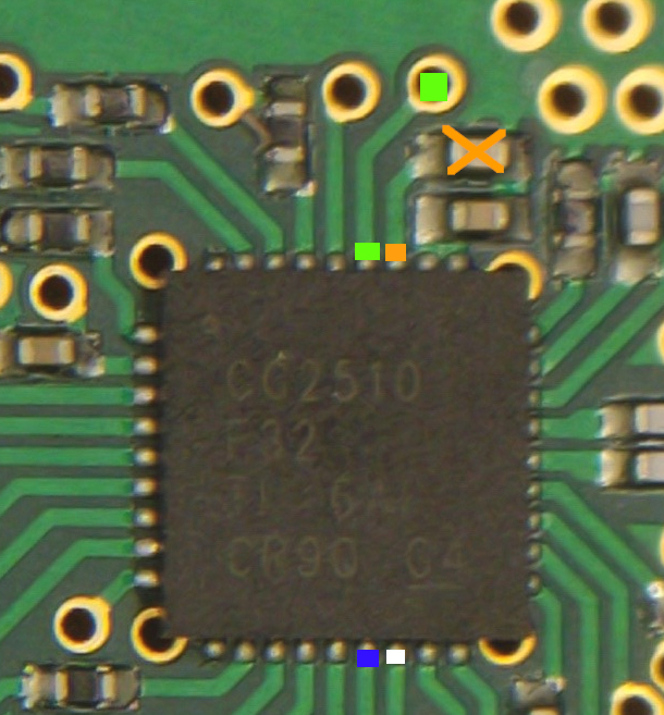
After gently prying apart the case, we got a closer look at the printed circuit board. This PCB had the e-ink screen and a battery connected to it. The battery was immediately disconnected before further work was done (as a safety precaution, to not accidentally short something). Pictures were then taken of the front and back of the PCB, see picture below for an explanation of the components.
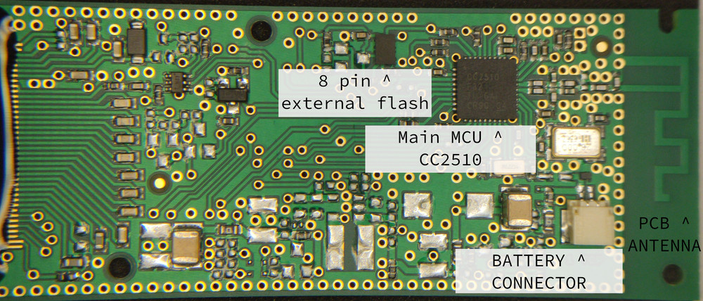
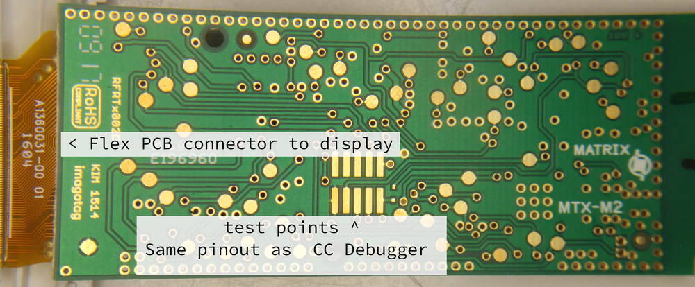
The product is an SES-imagotag G1 2.7 BW NFC, with product code B27N02003. On the PCB, there is some text: RFRTx002D and KIM 1514 (most likely internal part numbers), along with (most likely) a datecode: 09 17 (so September 2017). The PCB itself looks very professionally designed and made, with plenty of testpoints and programmer pads. Attached to the screen, there is an NFC tag which contains the ID of the board.
The board contains a CC2510 microcontroller. This microcontroller can communicate over 2.4GHz, and it’s clear that the product uses this feature: there is an antenna structure present on the PCB. It’s very likely that the image updates are done wirelessly via that antenna. The only remaining part is then to figure what the communication protocol looks like. Unfortunately, we don’t have the accompanying device that puts images on the screen, so intercepting the wireless communications wouldn’t be possible. What would be possible however, is reading the code from the microcontroller and seeing what it expects.
The pictures of the PCB were transformed and overlaid in GIMP. The front and back layers of the PCB were put in different GIMP layers, so that it would be easy to switch between different views without losing your frame of reference. When routing signals between places of the board, PCB designers sometimes have to use so-called ‘vias’ to move from the front of the board to the back of the board. From the marking ‘1 TOP’ and ‘4 BOT’ on the PCB, it became clear that this is 4-layer PCB: there are two visible layers, and two hidden layers sandwiched between them. Luckily, someone else used acid and sandpaper to make the hidden layers visible. This was however on a slightly different revision, but most components are in roughly the same position.
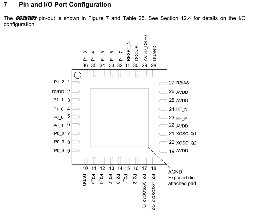
By reading the datasheet of the CC2510, it became clear that there is a debug interface. This interface can be used to put code on the board, to step through the code when debugging or even to read out the code. The debug interface consists of two signal pins: a host-to-microcontroller clock pin, and a bi-directional data pin. To enable the debug interface, the clock needs to be pulsed twice while the reset pin is held low. This makes for a total of 5 wires that need to be attached to the PCB: debug clock, debug data, reset; and then ground and 3.3V to power the board.
The CC2510 microcontroller contains an 8051 processor core. 8051 is a rather old 8-bit instruction set, originally made by Intel, but it is used in a lot of embedded products. The debug interface is quite ingenious in how it implements most features: instead of individually imlementing write, read, verify and other features, it has the DEBUG_INSTR instruction. This debug instruction takes one to three bytes of arguments, and executes these as an 8051 instruction. After that, it sends the value of the accumulator (ACC/A) register back over the debug interface. Reading out the memory then is a loop of setting an address we want to read out and moving the value at that address into the ACC register.
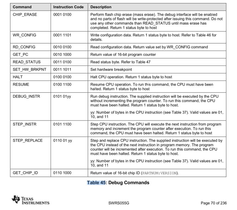
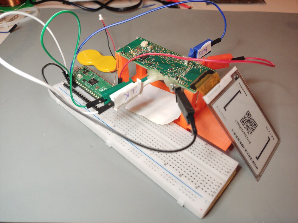
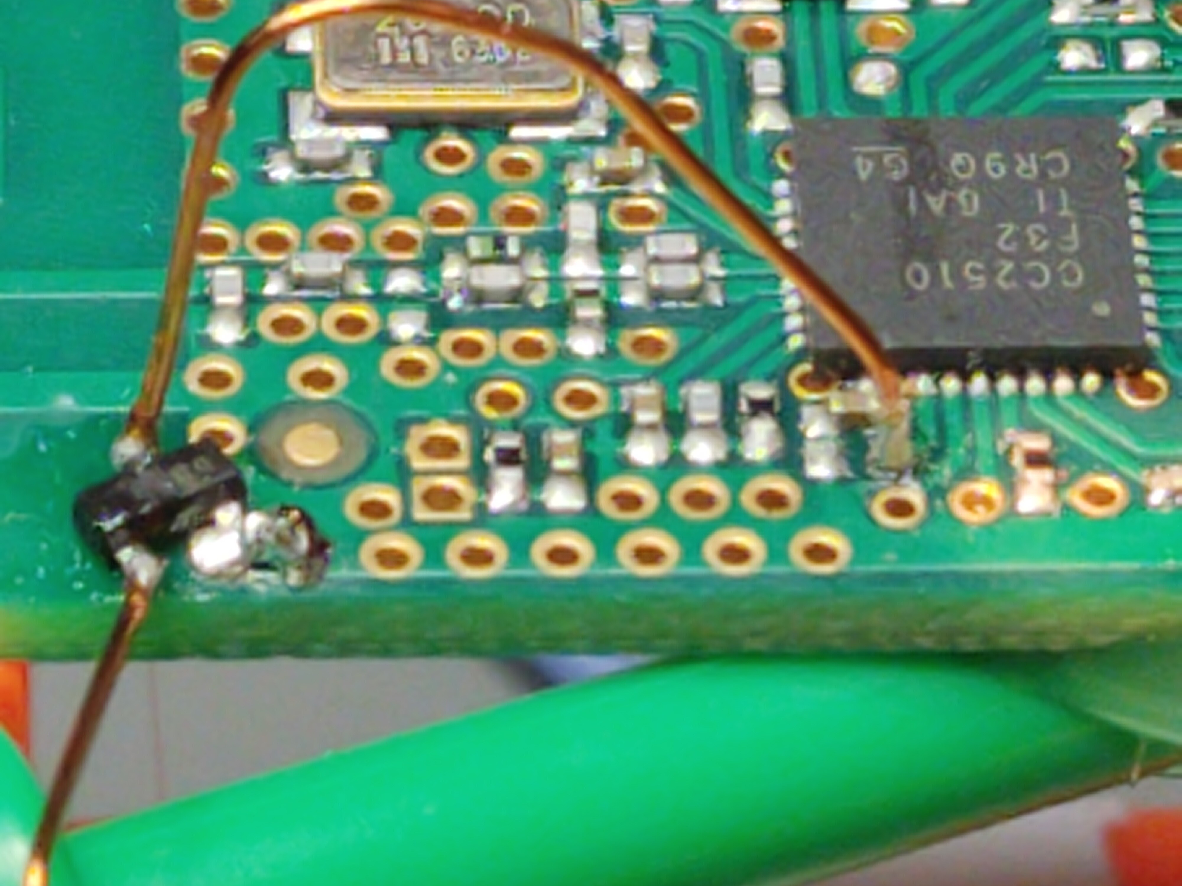
We attached the pins of the CC2510 to a Raspberry Pi Pico microcontroller and wrote a small application, based on ESP_CC_Flasher, to interface with debug interface of the microcontroller. Something unfortunate very quickly became clear: the chip was debug-locked: after programming the firmware on the microcontroller, the manufacturer disabled the debug interface. This means that only a very limited subset of debug instructions were enabled: only READ_STATUS (with which we can see, among others, if the chip is debug locked), GET_CHIP_ID (with which we can get the type of chip) and CHIP_ERASE (which erases the debug protection bits, but also all the other code). No instructions with which we can read out the board were found. Our new goal is thus to bypass the code read-out protection.
An initial idea was to issue the CHIP_ERASE command, and then immediately power off the board, hoping that the debug lock bits would be reset before the entire flash was wiped. This unfortunately didn’t work; I suspect that after issuing the CHIP_ERASE command, a bit gets written to flash indicating that an erase was requested, and that the startup sequence on the microcontroller checks this bit and then wipes the firmware until that bit is clear. I was a bit disappointed that I had wiped the board and thus bricked it, until I remembered the advise of bunnie to have a device you’ll never get working again. This wiped device later still came in useful as a development board to test other exploits against: I didn’t have to fear accidentally wiping or breaking the device, since it was already wiped.
After this initial setback, we tried another technique, namely voltage glitching. This is an exploit technique where you, for a very brief amount of time, change the voltage of the chip. This sometimes causes unexpected behaviour such as skipping certain instructions in a program or loading a different value from memory. The hope was that by voltage glitching at just the right time, we could bypass the debug lock and still execute a debug instruction that was disabled. To develop such an exploit, it’s critical to thoroughly read the datasheet of the chip, since this sometimes contains hints about how to proceed. In this case, several interesting parts were found:
Note that after the Debug Lock bit has changed due to a Flash Information Page write or a flash mass erase, a HALT, RESUME, DEBUG_INSTR, STEP_INSTR, or STEP_REPLACE command must be executed so that the Debug Lock value returned by READ_STATUS shows the updated Debug Lock value. For example a dummy NOP DEBUG_INSTR command could be executed. The Debug Lock bit will also be updated after a device reset so an alternative is to reset the chip and reenter debug mode.
This means that for every ‘interesting’ debug instruction, the chip probably first fetches the debug lock bit from flash and then checks if the command is allowed. For READ_STATUS, the value of the last debug instruction will be used. This is very useful for us: if we glitch a debug instruction, we’ll be able to see if we succeeded by issueing a READ_STATUS command. If it displays that the chip is unlocked, we’ll know that the previous instruction executed succesfully. This unfortunatly also means that for every debug instruction issued, we’ll have to succesfully glitch the board. This makes an exploit harder, because a voltage glitch has a high risk of rebooting the microcontroller, resetting our progress in the glitch. This means we’ll have to focus on reading out data with as few consecutive instructions that have to succeed as possible.
After inspecting the pinout, one pin, namely the DCOUPL pin, stood out:
DCOUPL: Power decoupling: 1.8 V digital power supply decoupling
The chip itself runs on 3.3V and no external pins have 1.8V logic level, so at first glance, it would be a bit strange for the chip to have a 1.8V power supply. However, this is actually rather common: the internal logic in the microcontroller (the CPU, RAM, flash, …) very likely uses 1.8V. The DCOUPL pin is meant to be attached to an external capacitor to smooth out the internal 1.8V power supply. For us, this is handy, because now we have a direct connection to the internal power supply.
To glich the microcontroller, we do some micro-surgery: we remove the decoupling capacitor and attach a fast MOSFET (a digital switch) to the DCOUPL and ground pin. When the MOSFET is enabled, the 1.8V power supply is shorted to ground, and the chip glitches. Succesfully mounting a voltage glitching attack then becomes a matter of correctly timing the glitch and closing the MOSFET for the right amount of time. Those timings need to be very precise, in the order of nanosecond precision. We basically need to pull a pin high for a very short time, at a very precise time in the debug sequence.
We previously used the Raspberry Pi Pico to communicate with the board; for the glitch timings, we’ll use the PIO (programmable IO) feature of the RP2040 chip on the Pi Pico. This cool piece of hardware allows us to set pins at the clock speed of the chip: so we can have a 125 MHz signal. We can feed the PIO peripheral using DMA (Direct Memory Access), so we can do other things while the glitch signal control runs in the background. The buffer that is used for the glich pin is thus filled with zeroes, except at one location, where there are a couple of consecutive ones.
A couple of modifications onto this idea were needed to make the attack more reliable:
- Overclocking the Pi Pico to 250 MHz instead of the default 125 MHz. This doubles the precision in glitch length and duration.
- The Pi Pico does its serial over software USB. The interrupts from USB sometimes throw off the timings, so we run the USB stack on core 0, and our code on core 1, with interrupts disabled.
- We set the drive strength of the power pin to 12 mA, and the slew rate to ‘fast’ (instead of the default ‘slow’). This makes sure that the internal capacitance of the MOSFET gate charges sufficiently fast, so we have a nice sharp edge on the glitch pin.
- We power-cycle the board after every glitch attempt, to reset it fully. This is done by connecting the 3.3V supply pin to a GPIO pin of the Pi Pico. The CC2510 microcontroller draws so little power that we don’t need a MOSFET for this, we can just directly power the board from that GPIO pin.
Now, a series of debug instructions needed to be constructed, with as few ‘forbidden’ instructions as possible, since every ‘forbidden’ instruction incurs the risk of rebooting the board. This came down to reading the 8051 instruction set, trying to find a series of instructions that load from a certain address into the accumulator register (the register sent back after every instruction). This ultimately was whittled down to two instructions:
MOV DPTR,#data16 (this loads a 16-bit constant into the DPTR/data pointer address)
MOVX A,@DPTR     (this loads the memory at DPTR into the accumulator register)
The full debug sequence is then, byte per byte:
-
DEBUG_INSTR, 3 bytes opcode argument -
MOV DPTR,#data16opcode -
#data16high byte -
#data16low byte - answer from microcontroller: accumulator register
READ_STATUS- answer from microcontroller: debug locked or not
-
DEBUG_INSTR, 1 byte opcode argument MOVX A,@DPTR- answer from microcontroller: accumulator register
READ_STATUS- answer from microcontroller: debug locked or not
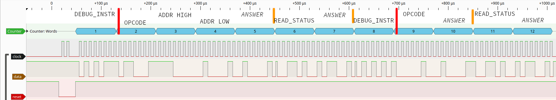
Using a parameter sweep accross the entire timing of the debug sequence and across glitch durations, a vulnerability was found in the DEBUG_INSTR: if we glitch the power supply right after DEBUG_INSTR, sometimes the debug lock is bypassed, resulting in execution of the DEBUG_INSTR and the correct accumulator answer. The next READ_STATUS instruction then also shows that the debug lock is unlocked. However, if we then execute another DEBUG_INSTR, the microcontroller will be locked again and it will fail. We thus need two succesful glitches to read out one byte of data, and we can know if our exploit executed succesfully by looking at the answers of READ_STATUS.
The parameters were then more finely tuned to optimize the chance of a succesful glitch. This tuning is very sensitive to parasitic elements: if the board is touched or moved even very slightly, the parameter tuning is off and the glitch parameters need to be recalibrated. The best success rate for a single glitch we’ve gotten is about 5%, but this quickly drops after running for an extended time, likely because of heating. Since a succesful glitch requires two successes, the success rate of reading a byte is 5% * 5% = 0.25% (if we assume both glitch chances are independent). We can do 35 attempts per second, so that results in about 1 byte read out every 20 seconds. Reading out the entire 32K flash would then take about 4 days. This attack was developed and tested against the wiped board and was verified to read out the correct data.
To make glitching more practical, the scripts were moved to a server in the Zeus WPI basement. Running the glitch scripts was done in a tmux session, so this attack could run in the background and we could remotely monitor it. After a couple of days, the readout rate considerably dropped and the parameters needed to be re-tuned.
Reading out the chip is rather slow: this is because our priorities for this exploit: first, to be cheap (the total cost of the hardware is about €10); and second to be simple and easy to reproduce. Some ways the success rate could be improved:
- More precise glitch timing and duration
- Connecting the MOSFET to ground (0V) likely is not the ideal voltage, a higher or lower short-circuit voltage is likely more efficient
- The glitch waveform is now a square wave. In this paper2, the authors propose arbitrary glitch waveforms and seem to get higher success rates as well
- Instead of voltage glitching, a different fault injection attack might also be succesful (for example clock glitching or electromagnetic fault injection)
Some other Texas Instruments RF chips use the same debugging protocol (ChipCon) and also have an embedded 8051 core. These chips have the part number CCxxxx. It’s likely that these chips are also vulnerable to the same attack. A non-exhaustive list:
- CC1110
- CC2430
- CC2431
- CC2510
- CC2511
This vulnerability was not explicitly reported to Texas Instruments, because they already have a security advisory that covers fault injection attacks against all chips: in TI-PSIRT-2021-100116 titled ‘Physical Security Attacks Against Silicon Devices’, published on January 31, 2022, it was stated in the ‘Affected products and versions’ section:
- If a TI product does not have documented mitigations against a specific physical attack, it may be vulnerable.
- If a TI product does have documented mitigations against a specific physical attack and a related vulnerability for that product is confirmed by TI, TI will publish a specific disclosure for that part.
This feels like a cheap cop-out where they say that basically every device is vulnerable unless they state otherwise, and they don’t even have to show this in the datasheet or in further security advisories, unless there is a mitigation for the exploit. Since it’s unlikely that there is a mitigation against this hardware attack without a silicon revision, TI probably wouldn’t even make a security advisory.
At the time of writing this blog post, 30.19% of the 32K flash memory of the e-ink tag has been read out. This memory was then loaded into Ghidra (a reverse engineering framework), where we confirmed that the dumped code is valid and sensible 8051 code. A next blog post will (hopefully) contain details about the reverse engineered protocol and how to talk with the e-ink tags. All exploit code is available in this repository.
Edit: reading out the entire memory took 6 days, so about 16 seconds per bytes, or 0.063 bytes per second. I think this might be the slowest bandwidth I’ve ever encountered.
Thanks pcy for answering my many questions and concerns about voltage glitching attacks.
2025-01-24 update: it turned out that one of the pages of the dump got corrupted (all 0xff bytes); I have since switched to working on another unrelated project (esp32-open-mac) and have not worked further on reproducing the attack again to get an uncorrupted page and be able to reverse engineer the firmware. For other people trying this attack: it would be good to create a custom PCB that has all the nescessary components needed to execute the glitching attack instead of modifying a regular PCB. This would make it a lot easier to swap in different microcontrollers in case one of the pages is corrupted.
If you have questions, comments or some things are not clear, feel free to email me zeusblog@notdevreker.be
-
The Hardware Hacker, by Andrew ‘bunnie’ Huang ↩
-
Bozzato, C., Focardi, R., & Palmarini, F. (2019). Shaping the Glitch: Optimizing Voltage Fault Injection Attacks ↩